- 您现在的位置:买卖IC网 > Sheet目录3882 > PIC16F87T-I/ML (Microchip Technology)IC MCU FLASH 4KX14 EEPROM 28QFN
LC88F83B0A
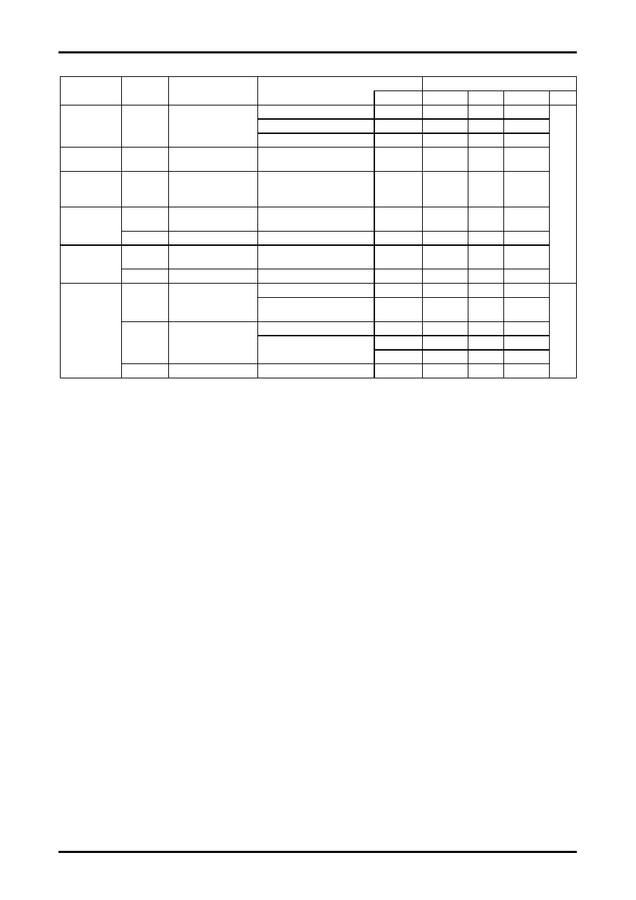
No.A1228-14/25
Allowable Operating Conditions at Ta = -20°C to +75°C, VSS = LCDVSS0 = LCDVSS1 = 0V
Parameter
Symbol
Pin
/Remarks
Conditions
Ratings
VDD[V]
min
typ
max
unit
Operating
supply voltage
(Note2-1)
VDD(1)
VDD
0.238
μs≤tCYC≤100μs
2.6
5.5
V
0.476
μs≤tCYC≤100μs
2.4
5.5
0.909
μs≤tCYC≤100μs
2.3
5.5
LCD drive
voltage
VLCD(1)
VLCD2 to VLCD4
5.5
Memory
sustaining
supply voltage
VHD
VDD
RAM and register contents
sustained in HOLD mode.
2.0
5.5
High level
input voltage
VIH(1)
Port 0, 1
Output disabled
0.30VDD
+0.70
VDD
VIH(2)
RESB
0.75VDD
VDD
Low level
input voltage
VIL(1)
Port 0, 1
Output disabled
VSS
0.10VDD
+0.40
VIL(2)
RESB
VSS
0.25VDD
Oscillating
frequency
range
(Note2-3)
FOSC0
XT1, XT2
Crystal oscillation
2.3 to 5.5
32.768
kHz
Low speed RC oscillation
(Note2-2)
2.3 to 5.5
30
80
FOSC1
CF1, CF2
Ceramic oscillation
2.4 to 5.5
400
4200
High-speed RC oscillation
(Note2-2)
2.4 to 5.5
400
4200
2.3 to 5.5
400
1100
FINTRC
Internal RC oscillation
1000
Note2-1: VDD must be held greater than or equal to 2.7V in the flash ROM onboard programming mode.
Note2-2: Ta=0
°C to 60°C
Note2-3: The parts value of oscillation circuit is shown in table 1 and table 2.
发布紧急采购,3分钟左右您将得到回复。
相关PDF资料
PIC16F87T-E/ML
IC MCU FLASH 4KX14 EEPROM 28QFN
PIC16F87-E/ML
IC MCU FLASH 4KX14 EEPROM 28QFN
PIC18LF4320-I/ML
IC MCU FLASH 4KX16 EEPROM 44QFN
PIC16F77T-I/PTG
IC MCU FLASH 8KX14 W/AD 44TQFP
PIC16LF1933-I/SO
IC PIC MCU FLASH 4K 28-SOIC
PIC16C54C-20I/SO
IC MCU OTP 512X12 18SOIC
PIC16LF726-I/SO
IC PIC MCU FLASH 8K 1.8V 28-SOIC
PIC12CE673-10/P
IC MCU OTP 1KX14 A/D&EE 8DIP
相关代理商/技术参数
PIC16F87T-I/SO
功能描述:8位微控制器 -MCU 7KB 368 RAM 16 I/O RoHS:否 制造商:Silicon Labs 核心:8051 处理器系列:C8051F39x 数据总线宽度:8 bit 最大时钟频率:50 MHz 程序存储器大小:16 KB 数据 RAM 大小:1 KB 片上 ADC:Yes 工作电源电压:1.8 V to 3.6 V 工作温度范围:- 40 C to + 105 C 封装 / 箱体:QFN-20 安装风格:SMD/SMT
PIC16F87T-I/SS
功能描述:8位微控制器 -MCU 7KB 368 RAM 16 I/O RoHS:否 制造商:Silicon Labs 核心:8051 处理器系列:C8051F39x 数据总线宽度:8 bit 最大时钟频率:50 MHz 程序存储器大小:16 KB 数据 RAM 大小:1 KB 片上 ADC:Yes 工作电源电压:1.8 V to 3.6 V 工作温度范围:- 40 C to + 105 C 封装 / 箱体:QFN-20 安装风格:SMD/SMT
PIC16F882-E/ML
功能描述:8位微控制器 -MCU 3.5KB Enh FLSH 128 RAM RoHS:否 制造商:Silicon Labs 核心:8051 处理器系列:C8051F39x 数据总线宽度:8 bit 最大时钟频率:50 MHz 程序存储器大小:16 KB 数据 RAM 大小:1 KB 片上 ADC:Yes 工作电源电压:1.8 V to 3.6 V 工作温度范围:- 40 C to + 105 C 封装 / 箱体:QFN-20 安装风格:SMD/SMT
PIC16F882-E/SO
功能描述:8位微控制器 -MCU 3.5KB Enh FLSH 128 RAM RoHS:否 制造商:Silicon Labs 核心:8051 处理器系列:C8051F39x 数据总线宽度:8 bit 最大时钟频率:50 MHz 程序存储器大小:16 KB 数据 RAM 大小:1 KB 片上 ADC:Yes 工作电源电压:1.8 V to 3.6 V 工作温度范围:- 40 C to + 105 C 封装 / 箱体:QFN-20 安装风格:SMD/SMT
PIC16F882-E/SP
功能描述:8位微控制器 -MCU 3.5KB Enh FLSH 128 RAM RoHS:否 制造商:Silicon Labs 核心:8051 处理器系列:C8051F39x 数据总线宽度:8 bit 最大时钟频率:50 MHz 程序存储器大小:16 KB 数据 RAM 大小:1 KB 片上 ADC:Yes 工作电源电压:1.8 V to 3.6 V 工作温度范围:- 40 C to + 105 C 封装 / 箱体:QFN-20 安装风格:SMD/SMT
PIC16F882-E/SS
功能描述:8位微控制器 -MCU 3.5KB Enh FLSH 128 RAM RoHS:否 制造商:Silicon Labs 核心:8051 处理器系列:C8051F39x 数据总线宽度:8 bit 最大时钟频率:50 MHz 程序存储器大小:16 KB 数据 RAM 大小:1 KB 片上 ADC:Yes 工作电源电压:1.8 V to 3.6 V 工作温度范围:- 40 C to + 105 C 封装 / 箱体:QFN-20 安装风格:SMD/SMT
PIC16F882-I/ML
功能描述:8位微控制器 -MCU 3.5KB Enh FLSH 128 RAM RoHS:否 制造商:Silicon Labs 核心:8051 处理器系列:C8051F39x 数据总线宽度:8 bit 最大时钟频率:50 MHz 程序存储器大小:16 KB 数据 RAM 大小:1 KB 片上 ADC:Yes 工作电源电压:1.8 V to 3.6 V 工作温度范围:- 40 C to + 105 C 封装 / 箱体:QFN-20 安装风格:SMD/SMT
PIC16F882-I/ML
制造商:Microchip Technology Inc 功能描述:IC 8BIT MCU PIC16F 20MHz QFN-28 制造商:Microchip Technology Inc 功能描述:IC, 8BIT MCU, PIC16F, 20MHz, QFN-28